Projects
Summary of Ongoing and accomplished projects:
1. Machine learning and Data Mining for Knowledge Discovery
Project 1.1. Deep Learning characterization of two-dimensional topological materials for enabling quantum sensing technology
Develop Predictive Models for New Topological Materials using Computational Data from First-Principles Calculations and Experimental Data of TM Synthesis and Characterization
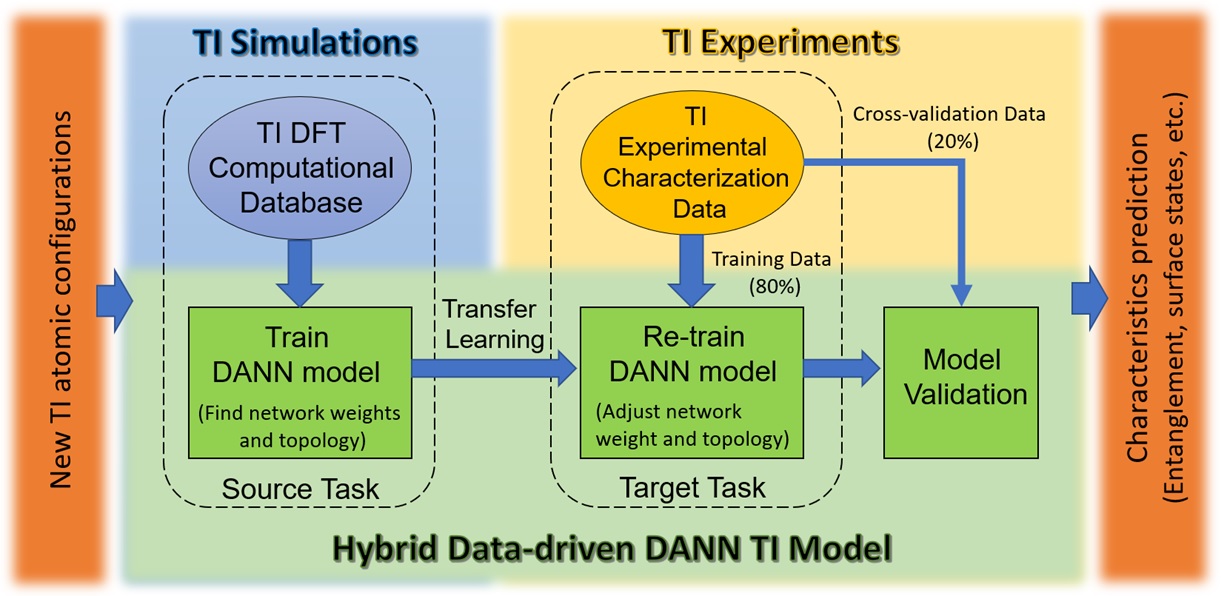
Figure: The flow chart of machine learning of topological insulators trained using the computational and experimental data.
Project 1.2. Harnessing Smart Additive Manufacturing using Machine Learning Techniques
Develop a closed-loop machine learning algorithm and improve the underling failure phenomena in laser-based 3D metal printing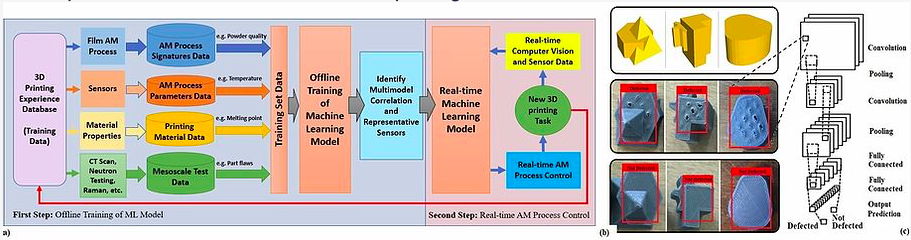
Figure: (a) Two-step strategy to establish the closed-loop machine learning algorithm for additive manufacturing process control; (b) Schematics of the objects in design software, corresponding printed parts with substantial defects on their surfaces that are detected and labelled by the CNN model as “defected” or “Not defected"; (c) Convolutional neural network procedure that extracts spatial features to pass to aggregation layers (averaging, pooling, etc.), followed by higher-order features extraction that is combined at the top layer for fault detection and classification.
Project 1.3. Identifying Laguerre-Gaussian Modes using Convolutional Neural Network
Develop an automated Determination of Laguerre-Gaussian (LG) modes to improve cavity tuning and optical communication.
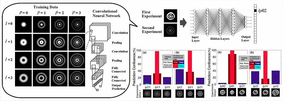
Figure: Training dataset of first 16 LG modes (l and p vary from 0 to 3) are passed to the CNN model that extracts spatial features using aggregation layers (averaging, pooling, etc.) and additional filter layers that are eventually combined at the top layer to predict and classify the new image of LG mode. Prediction confidence on two experimental setup of LG modes are also shown. The dark red and dark blue indicate the results of the CNN models trained using the simulated images while the light red and light blue indicate the results of the CNN models trained using both the simulated and experiment images.
Project 1.4. Enabling Fully Automated Analysis of Microscopy Images using CNN
Develop an architecture, fast and fully automated cell segmentation, classification and counting techniques for large scale high throughput microscopy images.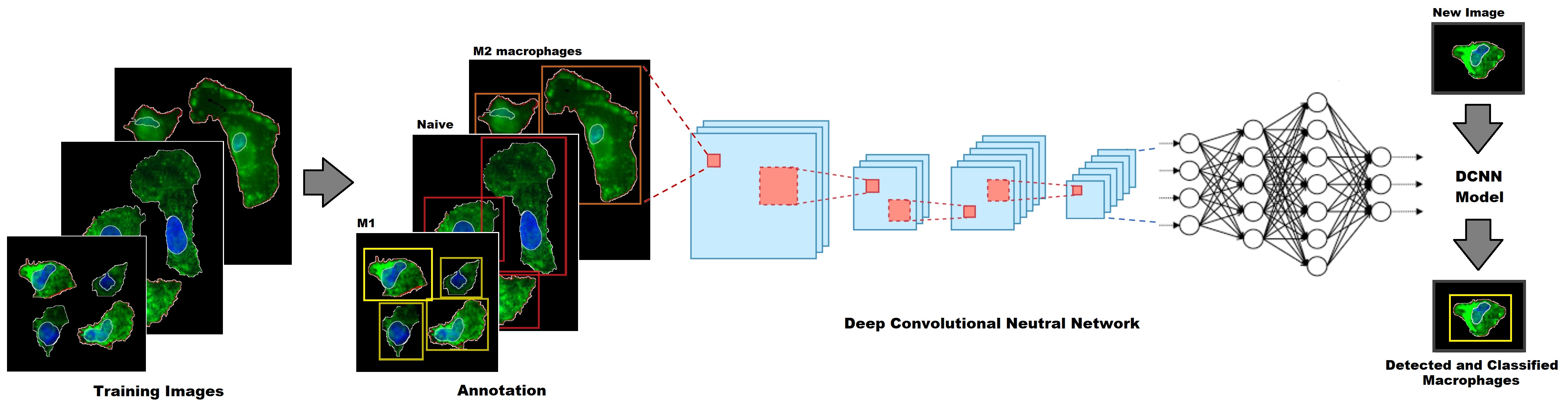
Figure: Preparation of samples and data sets of microscopy images, annotations by manually drawing bounding rectangles around cells associated with macrophages (identify polarized macrophages M1 and M2 phenotypes and distinguish them from unpolarized macrophages and monocytes), training CNN, and finally evaluation of the accuracy and performance of the framework by calculating precision, recall and F1 score of the cell counts and classifications to compare with the results of human experts and two other open-source software tools.
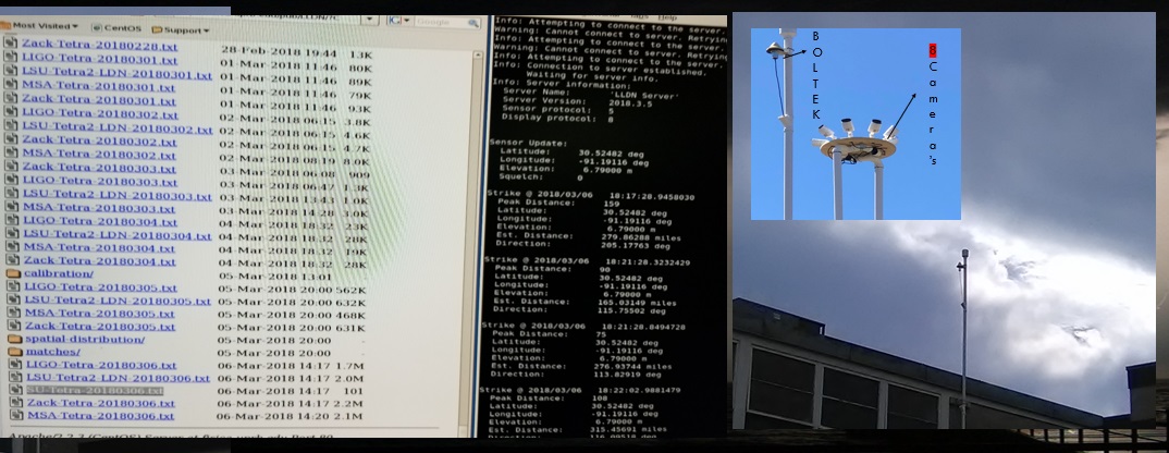
Project 1.5. Data-driven Analysis of Gamma-Ray Flashes Produced by Lightning Observed at Ground Level
Develop a data collection and interpretation algorithm to record bursts of gamma-rays of millisecond-scale duration associated with lightning strikes, analyze the pattern of events, and predict the thunderstorm characteristics.
2. Cyber Security and Intrusion Detection using Machine Learning Techniques
Project 2.1. Detecting Malicious DNS over HTTPS Traffic in Domain Name System using Machine Learning Classifiers
Develop a systematic two-layer approach for detecting DNS over HTTPS (DoH) traffic and distinguishing Benign-DoH traffic from Malicious-DoH traffic using six machine learning algorithms
Figure: (a) Training procedure of intrusion detection including data preprocessing, training, and optimizing the training algorithms, deployment of ML-based classifiers, and testing of the model to extract the classification performance metrics. (b) The network topology used to capture the traffic datasets, including benign and malicious DoH traffic along with non-DoH traffic.
Project 2.2. Design of Network Intrusion Detection Systems for the Internet of Things Infrastructure using Machine Learning Algorithms
Evaluating the performance of machine learning algorithms for network intrusion detection systems on the internet of things infrastructure.
Figure: (a) Training progress pipelines for four ML models: XGBoost classifier, random forest classifier, decision tree classifier, and gradient boosting classifier; (b) Classification measures of XGB classifier for four different sizes of attack datasets.
3. Computational Material Science for Emerging Sensing and Information Technology
Project 3.1. Graphene Nanostructure for Controlling Electromagnetic Fields
Introduce new graphene-based aperiodic multilayer structures as selective, tunable, and switchable thermal emitters at infrared frequencies.
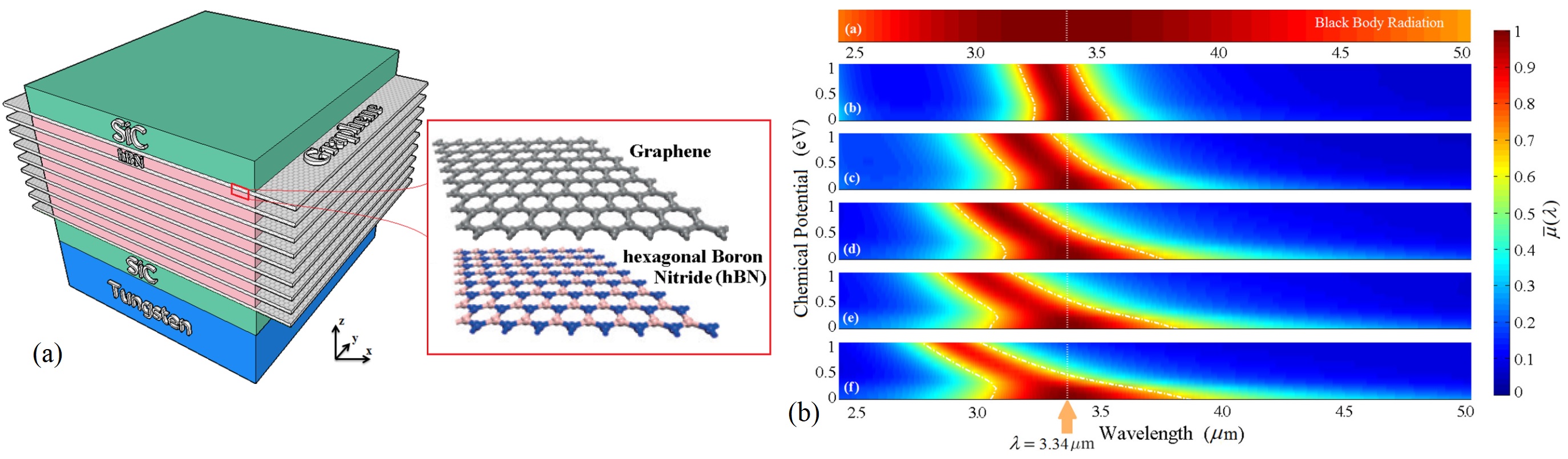
Figure: (a) Structure of the proposed thermal emitter composed of alternating layers of graphene and hBN insulator, which are sandwiched between two thick silicon carbide (SiC) layers. (b) Normalized thermal power emitted μ(λ) per unit area and unit wavelength in the normal direction from bulk tungsten versus wavelength and chemical potential at T = 873 K for the five optimized structures with 8, 13,23, 28, and 32 layers of graphene. The optimized graphene-based aperiodic multilayer structures enable narrowband thermal emission. The increase in the chemical potential results in a spectral shift toward shorter wavelength, enabling the electrically tunable thermal emitter, in which the range of tunability increases by increasing the number of graphene layers. The thermal emittance from the optimized structure with a larger number of graphene layers can be almost entirely eliminated by increasing the chemical potential so that perfect emittance of unity for the structure with 23 graphene layers can be switched to zero by setting μc equal to 1.0 eV.
Project 3.2. A Cost-Efficient Surface-Enhanced Raman Spectroscopy(SERS) Molecular Detection Technique for Clinical Applications.
Develop new techniques for Surface-Enhanced Raman Scattering (SERS) without costly and sophisticated fabrication steps.
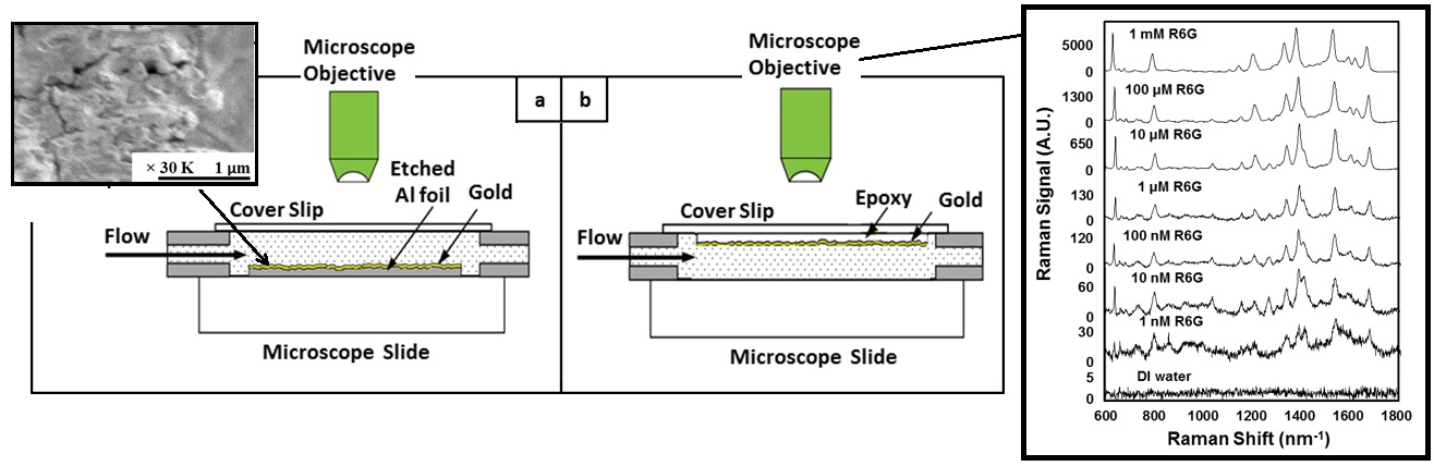
Figure: Test cells were filled with Rhodamine 6G. Laser light was focused on Au substrate on two cases by a 50 X microscope objective. (a) Au on etched aluminium foil (conventional view), (b) Au on UV epoxy (transmission view). Right figure shows Raman signals for gold on aluminium foil as a function of the concentration of Rhodamine 6G in DI water.
Project 3.3. Performance Evaluation of Graphene Transistor for Integrated Circuit Design
Study static metrics and switching attributes of graphene nanoribbon field-effect transistor (GNRFETs) using quantum transport model that self-consistently solves Poisson and Schrödinger equations within the non-equilibrium Green’s function (NEGF) formalism and fully treats on-parabolic band structure, short channel-length electrostatic effects and the quantum tunnelling effects in FET structures.
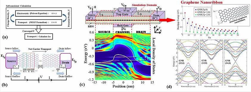
Figure: (a) Self-consistent calculation between electrostatic (Poisson equation) and transport (NEGF formalism) solutions. (b) Conceptual sketch of the armchair edge GNR channel including the quantities used in the NEGF formalism. (c) Energy-position-resolved local density of states of a typical GNRFET simulated with NEGF formalism, showing thermionic emission of carriers over the channel potential barrier, and the band-to-band-tunnelling of electrons from valence band in the channel region to the empty states in the drain side. (d) Bandgap energy of three GNR families of armchair GNR versus GNR index and energy dispersion relation of GNR(12,0), GNR(13,0) and GNR(14,0).
Project 3.4: A SPICE circuit model of graphene nanoribbon FET with edge roughness:
Develop a physics-based SPICE-compatible model for GNRFETs and the line-edge roughness of graphene that significantly degrades its performance such as an enhanced leakage current, reduced drive current, and increased threshold voltage.
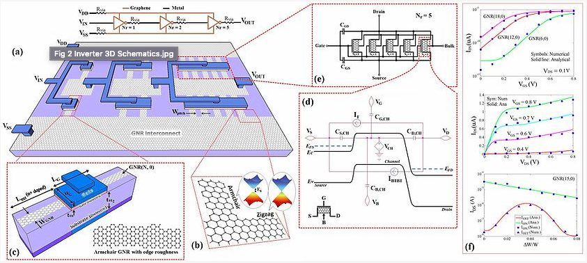
Figure: (a) 3D view of all-graphene circuit for an example of inverter chains together with its circuit implementation. The contact resistances of via connections are also shown corresponding to the layout design. (b) In all-graphene circuit, narrow armchair-edge GNRs and wide zigzag-edge GNRs are used as channel material and local interconnects, respectively. (c) 3D view of a GNRFET with one ribbon of armchair GNR(N,0) as channel material. (d) Energy band diagram and the corresponding components in the equivalent circuit model of a GNRFET with one GNR channel. (e) Circuit implementation of a GNR FET with multi-GNR channels consists of five nanoribbons connected to a wide zigzag GNR. (f) IDS–VGS characteristic of GNR FETs with three different GNR indices of N = 6, 12 and 18 for VDS = 0.1V, IDS–VDS characteristics of GNR FET at different gate voltages, and ON- and OFF- currents versus edge roughness amplitude ?W/W for LCH = 16 nm.
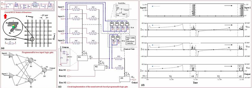
Project 3.5. Memristor as Synapsis in Neural Network Circuits:
Introduce a programmable logic gate using circuit implementation of artificial neural network and memristors, exotic electronic devices, only confirmed to exist in 2008.
Project 3.6. Graphene FET for Temperature Sensing Applications:
Introduce and evaluate graphene as a promising material for sensing and monitoring of die temperature at scaled bias voltages of emerging technology using semi-classical transport model incorporating different scattering mechanisms.
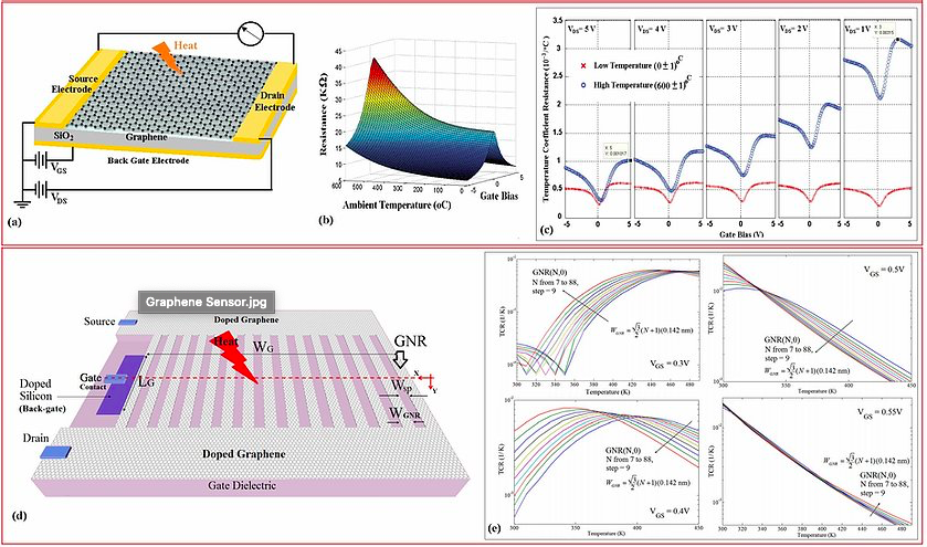
Figure 4. (a) Graphene field-effect transistor (G-FET) as a temperature sensor. (b) Resistance of G-FET versus temperature and gate bias at drain-source of 1V. (c) Temperature coefficient of resistivity (TCR) of the G-FET temperature sensor versus gate bias as a function of drain voltage of different drain-source voltage per Celsius degree variation. (d) Schematic diagram of the back-gate multi-channel graphene nanoribbon (GNR) FET temperature sensor device. (e) Temperature coefficient of resistance (TCR) measurements, illustrating the dependence on GNR width and gate bias.
Project 3.7. Carbon Nanotube Interconnects for Ionized Radiation detection:
Explore the feasibility of a carbon nanotube (CNT) ring oscillator (RO) for detecting ionized radiation using the displacement damage dose (DDD) methodology.
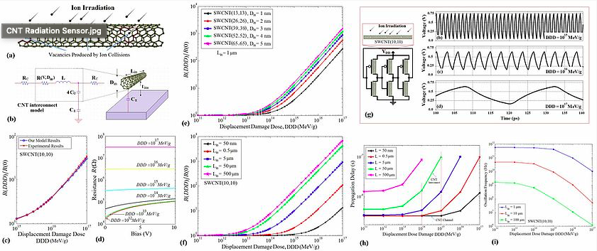
Figure 5. (a) Schematic of metallic CNT exposed to ionization radiation. (b) Transmission line model of a single-walled CNT interconnect. (c) Change in the ratio of the irradiated resistance, R(DDD) to the pre-irradiation resistance, R(0) as a function of increasing the displacement damage dose. (d) Total resistance versus voltage bias across 10µm length SWCNT (10,10) as a function of increasing DDD from 1012 MeV/g to 1017 MeV/g. The ratio of the irradiated resistance, R(DDD) to the pre-irradiation resistance, R(0) as a function of increasing the displacement damage dose for different (e) lengths and (f) diameter of SWCNT. (g) CNT-based ring oscillator consisting of six CNTFET and three CNT interconnects. Its output waveforms for exposure to ion radiation with three displacement density dose of 1015 MeV/g, 1016 MeV/g, and 1017 MeV/g. (h) The propagation delay of CNT inverter pair versus displacement damage dose for different CNT lengths. (i) The oscillation frequency of CNT-based RO versus DDD for metallic SWCNT (10,10) interconnects with three different lengths of 1 µm, 10 µm, and 100 µm.
Project 3.8. Power-efficient circuits design based on clocked adiabatic architecture in graphene FETs:
Introduce new energy-efficient gates based on clocked adiabatic logic (CAL) and graphene transistors.
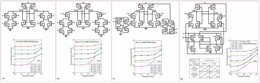
Figure 6. Circuit schematics of XNOR/XOR and the associated power density versus frequency for (a) 2N-2N2P design, (b) basic CAL design and (c) PL-GL CAL design, and (d) Low-Power CAL design.
Project 3.9. Resonant tunnelling diode for radio-frequency circuits design:
Develop a new large-signal SPICE model for RTD and evaluate its applications for a large signal oscillator, an RF amplifier and a frequency multiplier.
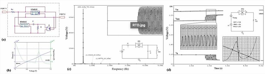
Figure 7. (a) The SPICE large-signal AC model of resonant tunnelling diode (RTD). (b) charge and capacitance versus the applied voltage across the diode. (c) Circuit schematic and output signal of RTD-based oscillator in time and frequency domains. (d) The input and output voltages of RTD-based amplifier at an optimum bias condition.
4. Quantum Computers and Optics
Project 4.1. Design of Microresonators to Minimize Thermal Noice Below Standard Quantum Limit.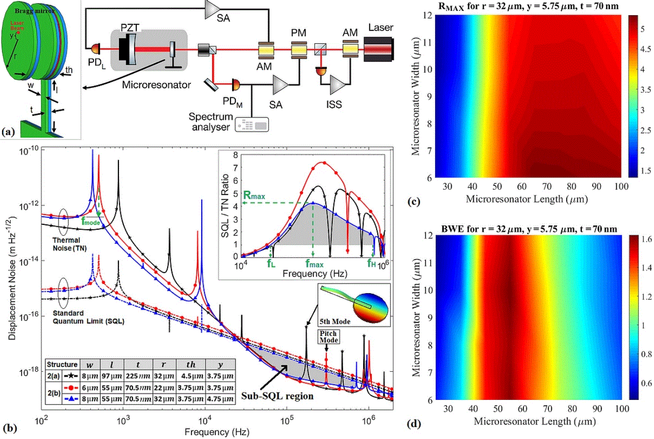
Figure 8. (a) Experimental arrangement of our optomechanical system and the optomechanical cavity consists of a macroscopic end mirror and a microresonator. (b) Thermal noise and standard quantum limit as a function of frequency for the microresonators, and the SQL/TN ratio for the microresonators, as well as the definition of the parameters. (c) RMAX and (d) BWE as a function of the lengths and widths of the optimized microresonators.
5. Computer Science Education for STEM
Project 5.1 Southern University - Computing and Data Education(Su-CoDE)


Website: www.subr.edu/page/gencyber
![]()
![]()
![]()